5.7 KiB
12/31/2025 4:21 AM - Selecting the microprocessor
Time spent: 0.7h
I started with selecting best Microcontroller
there are many MCU avalibable in market
but i select the ESP32-s3 because there Wide range of communication With Many protocols Including wifi and bLE Which made it a best choice.
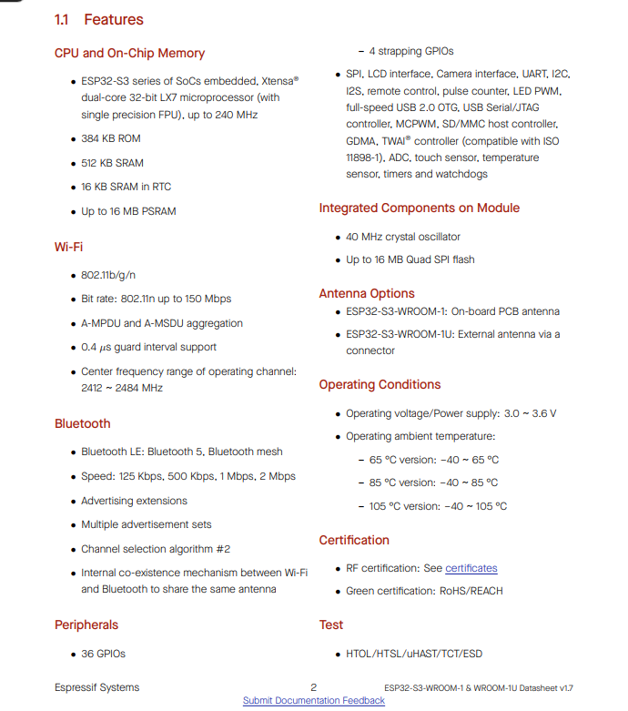 For more detail visit https://documentation.espressif.com/esp32-s3-wroom-1_wroom-1u_datasheet_en.pdf
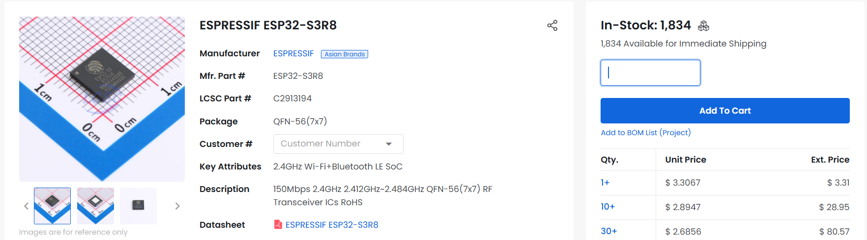
12/31/2025 4:25 AM - best deal
Time spent: 0.2h
It is easily available on Platforms like LCSC Electronics Which implies it can be easily assembled IN PCBA And second it is Only cost $3 something Which made them very Good MCU
12/31/2025 4:52 AM - Start designing Systematic
Time spent: 0.6h
So after finalising the microcontroller I start preparing I'm systematic
STARTING WITH ESP32-S3R8
 USE THE OFFICAL espressif DOCS
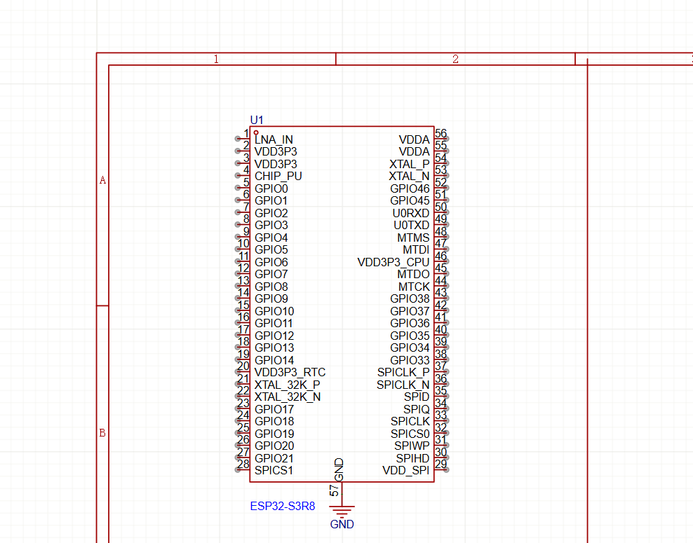
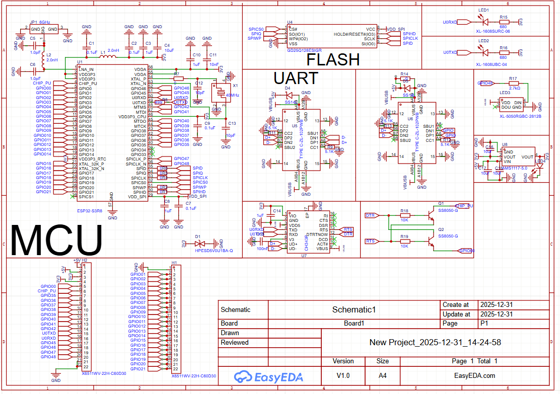
12/31/2025 6 AM - MCU CONNECTED
Time spent: 2.5h
FINALLY AFTER 2.3HOUR WORK THE MCU PINOUT, Timer Crystal CONNECTED AND POWER WIRING DONE
HERE IS IMAGE TO SHOW WHAT I DONE
 ALL THE MAIN MCU CONNECTION DONE
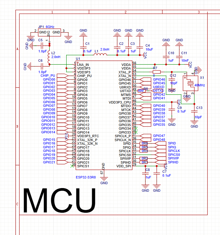
12/31/2025 10 AM - Flash memory and OTG Port
Time spent: 5.0h
Hi guys I'm not kidding it's 5 hour work
I unable to find the Flash memory used in ESP32 Anywhere ON DOCS
After 2.5 HR I decided to To remove the protective shield from my existing ESP32 Board and see what's there
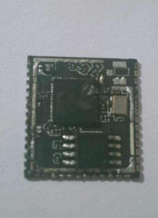
I Found that it consists of GigaDevice GD25Q128ESIG Flasher Memory
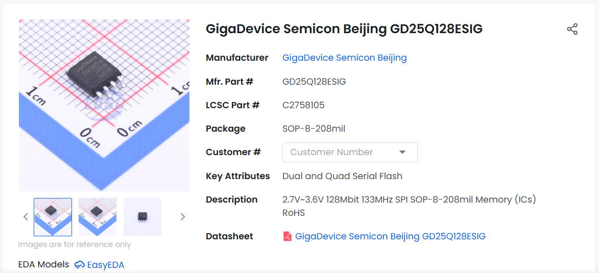 AND I ADD IT INTO THE Systematic
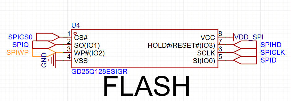 and made the connexion and I also added a The diode to protect it FROM Electronic spike And added to usb port One is for OTG and the second one is for Serial communication Otg part is done now I'm working on the serial communication.
12/31/2025 1 PM - Systematic done!
Time spent: 3.4h
Show after facing many issues I finally completed Systematic of the custom And It really difficult Because Some component Are not disclosed by the official Which I have to find And use it
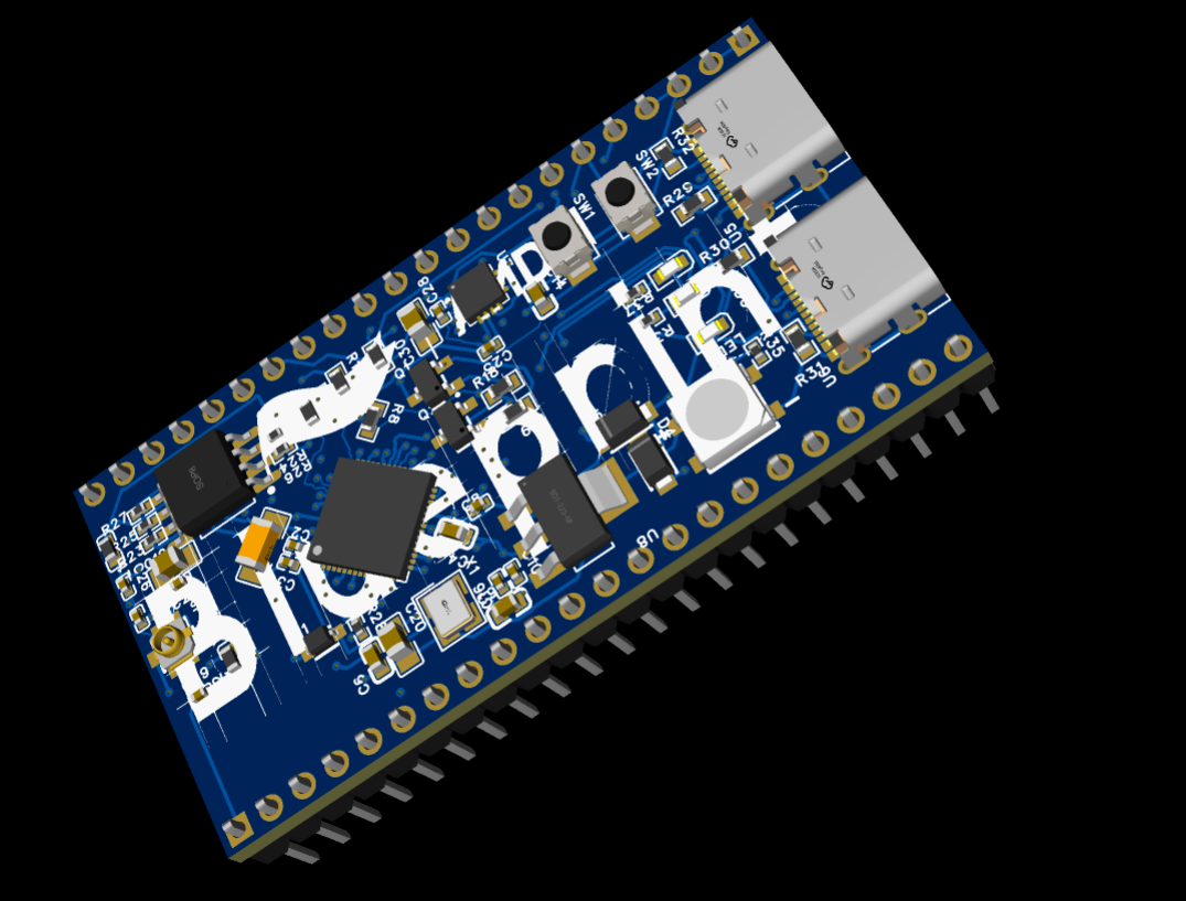
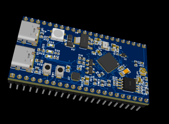
1/1/2026 4 AM - component placement
Time spent: 3.8h
So finally I completed The component placement And here's the image so you can take a look -
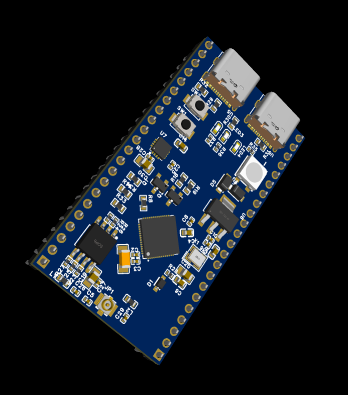
here is board
i know this process not take that much time but due to the compact size
Beginning of my PCB designing it take time
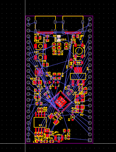
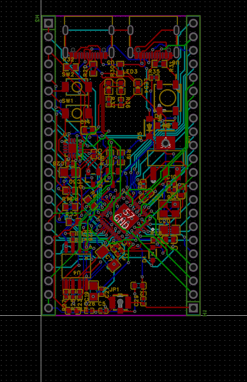
1/1/2026 3 PM - routed the pcb
Time spent: 6.3h
So what I in our previous post I place all the components on the place and he starte route And here's the good news all root is completed. Give a good round of applause to me
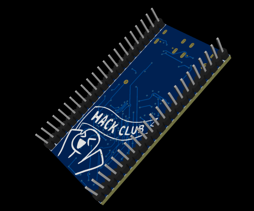
1/1/2026 4 PM - adding hackclub logo
Time spent: 0.4h
I added the hackclub logo on the pcb